Showing posts with label PCB Layout. Show all posts

Saturday, 5 May 2012

Low Cost 100W Inverter

Here is a 100 Watt inverter circuit using minimum number of components.I think it is quite difficult to make a decent one like this with further less components.Here we use CD 4047 IC from Texas Instruments for generating the 100 Hz  pulses  and four 2N3055 transistors for driving the load.
The IC1 Cd4047 wired as an astable multivibrator produces two 180 degree out of phase 100 Hz pulse trains.These pulse trains are  preamplifed by the two TIP122 transistors.The out puts of the TIP 122 transistors are amplified by four 2N 3055 transistors (two transistors for each half cycle) to drive the inverter transformer.The 220V AC will be available at the secondary of the transformer.Nothing complex just the elementary inverter principle and the circuit works great for small loads like a few bulbs or fans.If you need just a low cost inverter in the region of 100 W,then this is the best.


Notes.
  • A 12 V car battery can be used as the 12V source.
  • Use the POT R1 to set the output frequency to50Hz.
  • For the transformer get a 9-0-9 V , 10A step down transformer.But here the 9-0-9 V winding will be the primary and 220V winding will be the secondary.
  • If you could not get a 10A rated transformer , don’t worry a 5A one will be just enough. But the allowed out put power will be reduced to 60W.
  • Use a 10 A fuse in series with the battery as shown in circuit.
  • Mount the IC on an IC holder (socket).
  • Remember,this circuit is nothing when compared to advanced PWM inverters.This is a low cost circuit meant for low scale applications.
The maximum allowed output power of an inverter depends on two factors.The maximum current rating of the transformer primary and the current rating of the driving transistors.
For example ,to get a 100 Watt output using 12 V car battery the primary current will be ~8A ,(100/12) because P=VxI.So the primary of transformer must be rated above 8A.
Also here ,each final driver transistors must be rated above 4A. Here two will be conducting parallel in each half cycle, so I=8/2 = 4A .
These are only rough calculations and enough for this circuit.

Source: circuitstoday.com

See also about inverter
1. How to make a simple inverter
2. Inverter 100W with IC 4047

Monday, 30 April 2012

Charger Circuit Using LM 317 with Input 18V Battery

Here is a simple but effective battery charger circuit using IC LM 317.The circuit can be used to charge 12Vlead acid batteries.The circuit is very simple and can be easily assembled on a general purpose PCB.

The heart of the circuit is IC LM 317 ,which is an adjustable voltage regulator IC.The pin 1 of the IC is the control pin which is used to control the charging voltage.The pin 2 is the output pin at which the charging voltage appears.The pin 3 is the input pin to which the regulated DC supply is given.

The charging voltage and current is controlled by the Transistor Q1,resistor R1 and POT R5.when the battery is first connected to the charging terminals ,the current through R1 increases.This in turn increases the current and voltage from LM 317.When the battery is fully charged the charger reduces the charging current and the battery will be charged in the trickle charging mode.

Notes:
    * The input voltage to the circuit must be atleast 3V higher than the expected output voltage.LM 317 dissipates around 3V during its operation.Here I used 18V DC as the input.
    * The charging voltage can be set by using the POT R5.
    * The LM 317 must be mounted on a heat sink.
    * All capacitors must be rated atleast 25V.
    * You can use crocodile clips for connecting the battery to the charger.

Source : http://www.circuitstoday.com


Friday, 23 March 2012

Learn to Make USBasp is Easy

USB Downloader was made by Thomas Fischl. He used the the USB driver with  AVR that is being developed by Objective Development GmbH. USBasp consists of ATmega48 / 8 and a few passive components without requiring the other driver components. USBasp has several features such as:
  1. Can work on the Linux operating system, Mac OS X and Windows.
  2. Does not require a dedicated controller or SMD components.
  3. Programming speeds up 5Kbytes/sec.
  4. SCK option to support the target device with a low speed (<1.5 MHz)

Here I will help you to create your own USBasp with yourself.
Create a circuit USBasp as shown below with PCB software that you usually use. I use Eagle. (Click on the Picture to zoom in)
After the circuit schematic completed ,  convert to the form of PCB. Examples of  PCB results from the circuit above as:
Setting Hardware
Before the firmware is written to the microcontroller with USBasp, there are some hardware settings that need to be understood. There are three jumpers on the hardware used for configuration, they are:
  1. Jumper 1 (JP1) is used to provide 5V supply to the target through ISP connector. If the Jumper is connected, the target does not require any external supply because has been obtained from USBasp.
  2. Jumper 2 (JP2) is used to perform firmware upgrades. This jumper must be connected if you want to do the writing / frimware upgrade.
  3. Jumper 3 (JP3) connected with pin PC2 as the setting SCK. If the target has a lower clock speed (<1.5 MHz), then this jumper must be connected. SCK will be reduced from 375 kHz to 8 kHz.
Firmware Installation
USBasp made ​​in this post using ATmega8 microcontroller. The firmware can be installed using PonyProg 2000 with a parallel port interface. The steps to install the firmware is as follows:
  1. Connect the Jumper 2 (JP2).
  2. Connect USBasp  with PC / laptop via the USB port. When connecting this, there will be a warning " USB not recognize". Just ignore this warning.
  3. Load the firmware version used in accordance with the microcontroller. The firmware is contained in usbasp.2009-02-28\bin\firmware (download in   usbasp.2009-02-28.tar.gz 260 kB)or usbasp.2011-05-28\bin\firmware (download in usbasp.2011-05-28.tar.gz 519 kB).
  4. Set and setting H-Fuse L-fuse configuration for 12 MHz external crystal . For the ATmega8, H-fuse = 0xC9 and L-fuse = 0xEF, while for the ATmega48, H-fuse = 0xdd and L-fuse = 0FF. For the ATmega8, setting H-fuse and L-fuse  on PonyProg as follows:
  5. Click write to write the settings above.
  6. When finished, remove the back Jumper 2 (JP2) and unplug the USB cable.
Our work is not finished until here, one more step to complete.
Windows Driver Installation
  1. Connect USBasp  with laptop / PC using a USB cable.
  2. Will appear in Windows as shown below.
  3. Select "No, not this time", then press Next.
  4. Then select "Install from specific location (advanced)" and press Next.
  5. Then will appear,
  6. Navigate to the folder where the driver is located, that is, usbasp.2009-02-28 \ usbasp.2009-05-28 \ bin \ win_driver or usbasp.2011-05-28 \ usbasp.2011-02-28 \ bin \ win_driver (I use usbasp.2009-02-28 \ usbasp.2009-05-28 \ bin \ win_driver). In this folder there are two drivers folder. Which is is used depends on the WinAVR is used. If WinAVR that is used more than  2008-05-12, use libusb_0.1.12.1. If the version of WinAVR is used for longer, use libusb_0.1.10.1.
  7. Not long after, the installation process to be completed are marked with the appearance of the dialog box as shown below. Press Finish on this dialog box.
  8. To ascertain whether USBasp been installed properly, check through Device Manager. In the Device Manager will appear USBasp as shown below.
Download Firmware, Driver and Circuit
Software

Tuesday, 6 March 2012

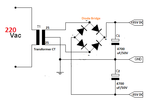
Symmetric Power Supply +35V and -35V Project

A symmetric power supply is needed when we make project about amplifier. Like an amplifier in sound system, it needs a symmetric power supply to operated. Here, we will construct a simple power supply circuit which result the output voltage is +35V and -35V.

This is the schematic and part of components


This project need a center-tap transformer, I recommend to use 3A transformer for good performances, 35 Amp of Diode Bridge for good rectifier, and 4700uF/50V Capacitor (If voltage of capacitor lower than output voltage, the capacitor will be explode, higher is better).
So this circuit is very simple, with 4 components you can construct a symmetric power supply.
NB:Be careful in the installation of components and wiring.

This is a proof of above project.


Related post :
12V Portable and Mobile Power Supply Circuit Diagram
Charger Circuit Using LM 317 with Input 18V Battery
The Working Principle of Power Supply
Power Supply +12V. -12V and +5V
MAKES A POWER SUPPLY 12V 5A

There are Power Supply Selections :


Monday, 27 February 2012

Minimum System of ATMEGA8

ATmega8 is a low power 8-bit microcontroller with RISC architecture. This microcontroller can execute a command dalah one period a clock for each instruction.
Some features of the ATmega8 are as follows:
1. 8 Kbyte Flash Program
2. 512 Kbyte EEPROM
3. 1 Kbyte SRAM
4. 2 8-bit timers and one 16 bit timer
5. Analog to digital converter
6. USART
7. analog comparator
8. Two wire interface (I2C)
Pin out of the ATmega8 can be seen in the following picture.

As we know, to make a usb downloader using ATMEGA8 we must have a minimum system of the uC. This circuit will help you to load the firmware to ATMEGA8.

This is the PCB layout of minimum system.
          Top view                                                                      Bottom view


NB : Value of the components are listed on the board and value of crystal is 8 - 12 Mhz

Thursday, 26 January 2012

AVR and The Minimum System

AVR is a microcontroller family which is now the most widely used. The concept of the AVR architecture was originally created by two students at Nerwegia Institute of Technology (NTH) that is Alf-Egil Bogen and Vegard Wallen which later developed by Atmel. Until now Atmel AVR family has issued few, the latter is a family of 32-bit RISC AVR. One family of AVR 8-bit microcontroller that is often used is ATMEGA8535/32.

That makes this microcontroller family of widely used people are :
  1. Have a Flash, a EEPROM, and a SRAM are all in one IC, so that in certain applications do not require external memory. 
  2. Program execution faster because nearly all instruction is conducted in only one or two clock cycles different with MCS-51, which performs instruction in 12 clock cycles. 
  3. Has many useful features, for example on ATMEGA8535, look at features
Click on the pictures to zoom in

The Minimum System of AVR


The minimum system circuit is a minimal circuit  where a microcontroller chip can work (running). Circuit is called minimal because of the use of hardware components that are used are the most minimal requirements for a processor to work. Actually AVR ATmega chip is equipped with an internal oscillator, so, to save costs (cost), no need to use a crystal / resonator external to source clock the CPU. But for good performance or we apply to projects that require a different oscillator with internal oscillator chip so we must use an external oscillator.
List of Components:


Name
Value
Quantity
uC (AVR)
ATMega8535/32
1
crystal
12Mhz
1
capacitors
30pF
2
elco
10uF
1
resistors
470
2
led

1
voltage regulator
LM7805
1
pin header
see pictures

If you have a downloader (serial or parallel), connect to the MISO. MOSI, SCK, RESET on the microcontroller (J1 in minimum system). Then to flash the program into the AVR  can use the software ISP flash-programmer v.30a. (free download)

Twitter Delicious Facebook Digg Stumbleupon Favorites More

 
Design by Free WordPress Themes | Bloggerized by Lasantha - Premium Blogger Themes | Bluehost Review