Tuesday, 10 July 2012

Infrared / Light Controled Switch

Description

This circuit is simple remote controlled relay. It is able to switch lamps or other devices.
D1 can be a phototransistor or LDR or an infrared transistor.
Circuit is controlled with an IR remote like a TV remote control (when IR transistor is used)
You can change circiut sensitivity with RV2.


Part List

U1:7805
U2:74111
U3:lm358
Rl1:5v relay
RV2:10k pot
R1:390R
R2:10k
D2:1n4007(for transistor projection)
C1:100uf 16V
C2:100uf 16V
Q1:TIPP112
J1:SIL2 conector for input power(circuit can work with 9V)
J2:terminal block M2

PCB

source : http://www.electronics-lab.com/projects/motor_light/026/index.html

Saturday, 7 July 2012

12V To 24V DC-DC Converter Circuit

This simple DC-DC converter can provide up to 24V from a 12V source. It can be used to run radios, small lights, relays, horns and other 24V accessories from a 12V vehicle with a maximum draw of about 800mA. It can be used to charge one 12V battery from another, or step up the voltage just enough to provide necessary overhead for a 12V linear regulator. Using one op-amp as a squarewave oscillator to ring an inductor and another op-amp in a feedback loop, it won't drift around under varying loads, providing a stable 24V source for many applications. With a wide adjustment in output this circuit has many uses.

Parts


Part


Total Qty.


Description


Substitutions
R1, R2, R3, R4, R8, R76100K 1/4W Resistor
R51470 Ohm 1/2W Resistor
R6110K Linear Pot
C110.01uF Mylar Capacitor
C210.1uF Ceramic Disc Capacitor
C31470uF 63V Electrolytic Capacitor
D111N4004 Rectifier Diode
D21BY229-400 Fast Recovery DiodeSee Notes
Q11BC337 NPN Power Transistor
U11LM358 Dual Op Amp IC
L11See Notes
MISC1Board, Wire, Socket For U1, Case, Knob For R6, Heatsink for Q1

Notes
  1. R6 sets the output voltage. This can be calculated by Vout = 12 x (R8/(R8+R7)) x (R6B/R6A).
  2. L1 is made by winding 60 turns of 0.63MM magnet wire on a toroidial core measuring 15MM (OD) by 8MM (ID) by 6MM (H).
  3. D2 can be any fast recovery diode rated at greater then 100V at 5A. It is very important that the diode be fast recovery and not a standard rectifier.
  4. Q1 will need a heatsink.
source :  www.aaroncake.net/circuits
Related Post :
1.2 - 36V / 5A Adjustable Power Supply
12V Portable and Mobile Power Supply Circuit Diagram
Charger Circuit Using LM 317 with Input 18V Battery

Power Supply Short Circuit Protection

Power Supply Short Circuit Protection


Description

This circuit designed to be used with:
0-30 Vdc Stabilized Power Supply With Current Control 0.002-3 A

Components values are shown in shematic.

Connect 741 +Vcc to D1 anode in main circuit
Connect 741 -Vcc to D3 catode in main circuit
U1 needs a 5v +Vcc connect pin 4 of U1 to 5v

Please note that +Vcc is above absolute maximum ratings of 741 which are +/- 22V, this may cause damage to OPAMP. You may need to add a LM7805 to power OPAMP. U1 needs at least 5v +Vcc.

Usage

- Power ON power supply then press START button to connect outputs to power supply.
- If output is shorted the relay disconnects output from power supply.
- Fix the short circuit and then press START again to connect output to power supply.

0-30 VDC STABILIZED POWER SUPPLY WITH CURRENT CONTROL 0.002-3 A

This is a high quality power supply with a continuously variable stabilized output adjustable at any value between 0 and 30VDC. The circuit also incorporates an electronic output current limiter that effectively controls the output current from a few milliamperes (2 mA) to the maximum output of three amperes that the circuit can deliver. This feature makes this power supply indispensable in the experimenters laboratory as it is possible to limit the current to the typical maximum that a circuit under test may require, and power it up then, without any fear that it may be damaged if something goes wrong. There is also a visual indication that the current limiter is in operation so that you can see at a glance that your circuit is exceeding or not its preset limits.

How it works

To start with, there is a step-down mains transformer with a secondary winding rated at 24 V/3 A, which is connected across the input points of the circuit at pins 1 & 2. (the quality of the supplies output will be directly proportional to the quality of the transformer). The AC voltage of the transformers secondary winding is rectified by the bridge formed by the four diodes D1-D4. The DC voltage taken across the output of the bridge is smoothed by the filter formed by the reservoir capacitor C1 and the resistor R1. The circuit incorporates some unique features which make it quite different from other power supplies of its class. Instead of using a variable feedback arrangement to control the output voltage, our circuit uses a constant gain amplifier to provide the reference voltage necessary for its stable operation. The reference voltage is generated at the output of U1.

The circuit operates as follows: The diode D8 is a 5.6 V zener, which here operates at its zero temperature coefficient current. The voltage in the output of U1 gradually increases till the diode D8 is turned on. When this happens the circuit stabilizes and the Zener reference voltage (5.6 V) appears across the resistor R5. The current which flows through the non inverting input of the op-amp is negligible, therefore the same current flows through R5 and R6, and as the two resistors have the same value the voltage across the two of them in series will be exactly twice the voltage across each one. Thus the voltage present at the output of the op-amp (pin 6 of U1) is 11.2 V, twice the zeners reference voltage. The integrated circuit U2 has a constant amplification factor of approximately 3 X, according to the formula A=(R11+R12)/R11, and raises the 11.2 V reference voltage to approximately 33 V. The trimmer RV1 and the resistor R10 are used for the adjustment of the output voltages limits so that it can be reduced to 0 V, despite any value tolerances of the other components in the circuit.
Schematic diagram
Another very important feature of the circuit, is the possibility to preset the maximum output current which can be drawn from the p.s.u., effectively converting it from a constant voltage source to a constant current one. To make this possible the circuit detects the voltage drop across a resistor (R7) which is connected in series with the load. The IC responsible for this function of the circuit is U3. The inverting input of U3 is biased at 0 V via R21. At the same time the non inverting input of the same IC can be adjusted to any voltage by means of P2.

Let us assume that for a given output of several volts, P2 is set so that the input of the IC is kept at 1 V. If the load is increased the output voltage will be kept constant by the voltage amplifier section of the circuit and the presence of R7 in series with the output will have a negligible effect because of its low value and because of its location outside the feedback loop of the voltage control circuit. While the load is kept constant and the output voltage is not changed the circuit is stable. If the load is increased so that the voltage drop across R7 is greater than 1 V, IC3 is forced into action and the circuit is shifted into the constant current mode. The output of U3 is coupled to the non inverting input of U2 by D9. U2 is responsible for the voltage control and as U3 is coupled to its input the latter can effectively override its function. What happens is that the voltage across R7 is monitored and is not allowed to increase above the preset value (1 V in our example) by reducing the output voltage of the circuit.

This is in effect a means of maintaining the output current constant and is so accurate that it is possible to preset the current limit to as low as 2 mA. The capacitor C8 is there to increase the stability of the circuit. Q3 is used to drive the LED whenever the current limiter is activated in order to provide a visual indication of the limiters operation. In order to make it possible for U2 to control the output voltage down to 0 V, it is necessary to provide a negative supply rail and this is done by means of the circuit around C2 & C3. The same negative supply is also used for U3. As U1 is working under fixed conditions it can be run from the unregulated positive supply rail and the earth.

The negative supply rail is produced by a simple voltage pump circuit which is stabilized by means of R3 and D7. In order to avoid uncontrolled situations at shut-down there is a protection circuit built around Q1. As soon as the negative supply rail collapses Q1 removes all drive to the output stage. This in effect brings the output voltage to zero as soon as the AC is removed protecting the circuit and the appliances connected to its output. During normal operation Q1 is kept off by means of R14 but when the negative supply rail collapses the transistor is turned on and brings the output of U2 low. The IC has internal protection and can not be damaged because of this effective short circuiting of its output. It is a great advantage in experimental work to be able to kill the output of a power supply without having to wait for the capacitors to discharge and there is also an added protection because the output of many stabilized power supplies tends to rise instantaneously at switch off with disastrous results.  

Parts List

R1 = 2,2 KOhm 1W
R2 = 82 Ohm 1/4W
R3 = 220 Ohm 1/4W
R4 = 4,7 KOhm 1/4W
R5, R6, R13, R20, R21 = 10 KOhm 1/4W
R7 = 0,47 Ohm 5W
R8, R11 = 27 KOhm 1/4W
R9, R19 = 2,2 KOhm 1/4W
R10 = 270 KOhm 1/4W
R12, R18 = 56KOhm 1/4W
R14 = 1,5 KOhm 1/4W
R15, R16 = 1 KOhm 1/4W
R17 = 33 Ohm 1/4W
R22 = 3,9 KOhm 1/4W
RV1 = 100K trimmer
P1, P2 = 10KOhm  linear potentiometer
C1 = 3300 uF/50V electrolytic
C2, C3 = 47uF/50V electrolytic
C4 = 100nF polyester
C5 = 200nF polyester
C6 = 100pF ceramic
C7 = 10uF/50V electrolytic
C8 = 330pF ceramic
C9 = 100pF ceramic
D1, D2, D3, D4 = 1N5402,3,4 diode 2A - RAX GI837U
D5, D6 = 1N4148
D7, D8 = 5,6V Zener
D9, D10 = 1N4148
D11 = 1N4001 diode 1A
Q1 = BC548, NPN transistor or BC547
Q2 = 2N2219 NPN transistor
Q3 = BC557, PNP transistor or BC327
Q4 = 2N3055 NPN power transistor
U1, U2, U3 = TL081, operational amplifier
D12 = LED diode
source : http://www.electronics-lab.com/projects/power/001/index.html
Related post:
1.2 - 36V / 5A Adjustable Power Supply
12V Portable and Mobile Power Supply Circuit Diagram
Charger Circuit Using LM 317 with Input 18V Battery

Friday, 6 July 2012

1.2 - 36V / 5A Adjustable Power Supply

Description

This is a very simple and adjustable voltage power supply. Max input voltage is 37V and output adjustable between 1.2 to (vcc - 3) volts.

Q1 is a power PNP Darlington transistor and is used to boost current of  LM317. It's the most useful adjustable regulator and for this circuit you can also use LM317L thats can give 100mA, thats enough for transistor bias.

D1 and D2 are protection diodes because when you turn the circuit off the output capacitors discharing and can damage the transistor or regulator.

R1 is 2W and other resistors are 0.25W

R1 is LM317 current limiting resistor and R2 is Q1 bias resistor all capacitors are 50V RV1 is 5k multi turn volume pot.

100nf capacitors are in parallel with electrolytic capacitors to remove high frequency noise because large value electrolytic have large ESR and ESL and cant remove high frequency noise.

I will design a pcb for this circuit and add to project .

Q1 need heatsink and small fan.
Circuit maximum output is 125W
source : http://www.electronics-lab.com/projects/power/021/index.html
Related Post:
12V Portable and Mobile Power Supply Circuit Diagram
Charger Circuit Using LM 317 with Input 18V Battery

PIR Motion Sensor and Schematic Diagram

Introduction

The objective of this project is to use inexpensive PIR sensor to detect if a human has moved. To build this project I use a PIC18F25K20 microcontroller to detect if the sensor had change state and it will emit a sound from the speaker or piezo, the MCU also detect the voltage of the battery in the startup, the algorithm it´s very simple it use an interrupt on change to detect the change on the PIR sensor.


PIR Sensor

PIR sensors allows you to sense motion, almost always used to detect whether a human has moved in or out of the sensors range. They are small, inexpensive, low-power, easy to use and don't wear out. For that reason they are commonly found in appliances and gadgets used in homes or businesses. PIRs are basically made of a pyroelectric sensor, which can detect levels of infrared radiation. Everything emits some low level radiation, and the hotter something is, the more radiation is emitted. The sensor in a motion detector is actually split in two halves. The reason for that is that we are looking to detect motion (change) not average IR levels. The two halves are wired up so that they cancel each other out. If one half sees more or less IR radiation than the other, the output will swing high or low.
Schematic

 Part List
Power Supply


I use a 9V battery and it´s connect to a switch and as a voltage regulator I use an L317T and it will have an output of 3,3V to make that possible I use two resistors R1 and R2 to set the output, i use this equations to calculate R1 and I set R2 to 240 ohms:
POR (Power on reset)

I had to add a RC delay on VPP pin because when I switch on/off the circuit there was a voltage drop because the PIR Sensor and that would generate an unknown state when the MCU was restarted to solve that I add a RC delay, you can use this equations to calculate the delay
Speaker or Piezo

I use an 8 ohm speaker but you can use a piezo, i use a transistor BC338 (Q1) because the sound wasn´t too loud and should be able to ear that from a different division, with that transistor i get a HFE = 35. You can calculate ic with this equation.
PIR Sensor

This PIR Sensor works with only 3.3V like the MCU so it´s connect to the output of LM317T it can be connect to a voltage of 8V to 24V, because I use a 9V battery and if the battery gets lower than 8V the PIR sensor won’t work that is why I connect the output of LM317T. The Vout of the sensor it is connected to PORTB.0 and when it occurs a change it will cause an interrupt I use a pull down resistor to make sure the PORTB.0 it is in a low state. The sensor takes 10 to 12 seconds to cause another interrupt and the range is between 2m and 3m. There are the graphs of this sensor and the delays.
Algorithm

At startup both LEDs are on and then it will test the battery if is good Led1(Green) will switch on/off three times, if battery it is low Led2(Blue) will switch on/off three times, next it will put the Led1(Green) on, if PORTB.0 doesn´t change state the circuit will remain the same until a change happen and when a change happen it means the sensor detects some movement and a interrupt will occur and Led1 will be turn off and Led2 will be on and a sound will be generate during 5 seconds and then Led2 will switch off and return to the main routine.
Download Source Code in hex
source : http://www.electronics-lab.com/projects/sensors/007/index.html
Related post:
How do motion sensing lights and burglar alarms work?

Thursday, 5 July 2012

How To Build a Laser Security System

Got a mystery to solve? Somebody’s been making off with your stuff, and you don’t have a clue who it is, do you? Here’s your chance to catch them in the act.

To make a laser security system you will need:

    A laser pointer
    Some Duct tape
    A few small mirrors
    An L.M.741 microchip
    A 220-ohm resistor
    A photocell
    An inexpensive digital camera
    An extra small screwdriver
    A wire coat hanger
    Some thin, insulated wire
    A printed circuit board
    A 9 volt battery
    A 9 volt battery clip
    Soldering equipment
    A pair of wire cutters
    A soap caddy with drainage holes
    A voltage relay

Step 1
Build the circuit

Build the circuit. Center the microchip on the circuit board. Pop in the voltage regulator. Connect the battery clip leads to the regulator. Run 2 more leads out from the regulator. Pop in the resistor and the photo cell. Link the chip to the photo cell. Pop in the relay. Link the chip to it as well. Link the other side of the relay to "power."

Step 2
Disassemble camera

Disassemble the digital camera so you can access the board connected to the camera’s trigger button.

Tip
You may have to remove the camera’s board to get a good solder point on the terminal.

Step 3
Solder wires to terminals

Look for the two tiny terminals that lead to the trigger button. Solder wires to each of these terminals and feed them through the trigger button hole.

Step 4
Reassemble the camera

Reassemble the camera. If you can’t get it back together easily, use duct tape to keep it closed. Just don’t tape over the lens.

Step 5
Position circuit inside soap caddy

Position the circuit inside the soap caddy so the photocell is exposed behind one of the holes.

Step 6
Connect battery to circuit

Connect the battery to the circuit, and use tape to secure the whole assemblage inside the box.

Step 7
Attach wires to voltage relay

Slip the two wires coming from the camera through another hole, and attach them to either side of the voltage relay.

Step 8
Cut & tape coat hangers

Cut the coat hanger into several pieces. Tape one piece to the laser pointer and the others to the back of the mirrors.

Step 9
Place camera

Place the camera in an inconspicuous location with the lens pointing at the object you want to protect and secure it in place.

Step 10
Position laser pointer

Position the laser pointer in another inconspicuous place and secure it too.

Step 11
Place mirrors

Place the mirrors to create a perimeter around the object you’re protecting, adjusting them until the laser hits the photocell.

Step 12
Test the system

Now break the beam to test the system… And get ready to confront the perpetrator with your irrefutable evidence.

Fact

The term LASER is really an acronym for Light Amplification by Stimulated Emission of Radiation.
source :  http://www.howcast.com/videos/2947-How-To-Build-a-Laser-Security-System
Related post :
Car Alarm System

Wednesday, 4 July 2012

Water Alarm Circuit

Project Summary

this circuits remember us that our tank is near about to get full so that we turn off our motor switch but for this circuit you need a function generator specially

Project Description

This circuit gives out an alarm when its sensor is wetted by water. A 555 astable multivibrator is used here which gives a tone of about 1kHz upon detecting water. The sensor when wetted by water completes the circuit and makes the 555 oscillate at about 1kHz.
The sensor is also shown in the circuit diagram. It has to placed making an angle of about 30 – 45 degrees to the ground. This makes the rain water to flow through it to the ground and prevents the alarm from going on due to the stored water on the sensor. The metal used to make the sensor has to be aluminium and not copper. This is because copper forms a blue oxide on its layer on prolonged exposure to moisture and has to be cleaned regularly. The aluminium foils may be secured to the wooden/plastic board via epoxy adhesive or small screws. The contact X and Y from the sensor may be obtained by small crocodile clips or you may use screws
source : http://www.eeweb.com/project/ervindhya_vasini_manath_mahajan/water-alarm
Related post :
Car Alarm System


300 Watt MOSFET Real HI-FI Power Amplifier

Project Summary

My passion for excellence progressed over the past 40 years to developing sonically superior amplifiers to the highest possible standards, providing life like sound performance.

Project Description
 Figure 1
I am committed to sharing my experience of the RAS 300 with other enthusiasts sharing my passion for perfection.I designed this minimalist amplifier to be durable, simple to operate while offering high fidelity equivalent to the original sound source and would recommend partnering this amplifier only with other products of outstanding quality.

When I set out to design this amplifier, my aim was to create a product most suitable for the reproduction of complex music and speech signals. Although I placed high emphasis on electrical characteristics, the single most important requirement is achieving an audibly superior sound, vivid spatial imaging and superb tonal clarity.

Although the average listening level is normally less than 10 watts, my design approach was to create an amplifier with ample reserve power, but biasing it for class A at average listening levels reducing cross-over distortion to extremely low levels.

There is not one capacitor in the signal path, improved the accuracy of the tonal characteristics of instruments and voices significantly.
The RAS 300 has almost zero phase distortion far beyond the audio range resulting in perfect resolution and totally un-coloured sound.

Amplifier Specification:
Maximum Output: 240 watts rms into 8 Ohms, 380 watts rms into 4 Ohms
Audio Frequency Linearity: 20 Hz – 20 kHz (+0, -0.2 dB)
Closed Loop Gain: 32 dB
Hum and Noise: -90 dB (input short circuit)
Output Offset Voltage: Less than 13 mV (input short circuit)
Phase Linearity: Less than 13 0 (10 Hz – 20 kHz)
Harmonic Distortion: Less than 0.007% at rated power
IM Distortion: Less than .009% at maximum power

The amplifier consists of two completely separate monaural amplifiers each channel has its own power supply, resulting in zero inter-channel cross talk, a common phenomenon in amplifiers sharing the same power supply.

In order to obtain the full output power each supply transformer should be rated at 40VAC – 0 – 40VAC at 640VA. Unlike many designs relying on the reservoir capacitors to supply peak currents, I prefer to have the raw power available from the transformer resulting in much faster transients.

Although the RAS 300 specifications are moderate, when listening to it you will immediately experience the massive reserve power available and never have any cause of anxiety that something is going to give in that one would when driving many amplifiers loud.

You will hear nothing but reality with no distortion at any level and I guarantee that this amplifier will divulge the best qualities of any equipment connected to it.
source :http://www.eeweb.com/project/circuit_projects/300-watt-mosfet-real-hi-fi-power-amplifier
Project Files

File NameFile Size
PCB layouts and parts files376.57 KB
Related Post:
A Simple 50W Amplifier Circuit
RA53 Stereo Headphone Amplifier Connection Schematic
TDA7360 Stereo Test and Application Circuit Diagram and Datasheet

Car Alarm System

Project Summary

The project is almost acceptable of a car alarm system, which could be completed with a transmitter and receiver.
Project Description

This project is practical, and the hex file, it can get. Button switch to disable the system. Button to open the door for when the driver enters the cars, and system deactivates the trigger button, if starter switch is closed, the device is completely passive. In this mode, only open or close doors button can be used.
proteus 7.8 or 7.9

Project Files
File NameFile Size
hex14.43 KB

 source : http://www.eeweb.com/project/abba_ba/car-alarm-system

Tuesday, 3 July 2012

TDA7360 Stereo Amplifier Test and Application Circuit Diagram and Datasheet

Car radio application using class AB Audio Power Amplifier usually has TDA7360 inside it. It is a 22W bridge or stereo audio ampwith features such as minimum external components, high output power, fixed gain, clipping detector and etc.
Above circuit diagram shows this TDA7360 stereo test and application circuit schematic. Value recommendation of each external components of this circuit can be described as follows: 1. C1 for input decoupling (CH1) is 0.22 uF
2. C2 for input decoupling (CH2)3is 0.22 uF
3. C3 for supply voltage rejection filtering capacitor.
4. C4 for 22uF standby ON/OFF delay
5. C5 minimal 220uF for standby-pass
6. 100 nF for C6 with its ability to supply by-pass
7. 2200 uF for the C7 of Output decoupling CH2

The TDA7360 bridge/stereo audio amplifier datasheet in pdf filetype may give you complete explanation.

Related post:
A Simple 50W Amplifier Circuit
RA53 Stereo Headphone Amplifier Connection Schematic

RA53 Stereo Headphone Amplifier Connection Schematic

This stereo headphone amplifier device may provide up to ten channels of headphone monitoring if a 1/4” Link Input/Output jack is provided for connecting two RA53 units together. The schematic below illustrates a possible operation for this RA53 stereo headphone amplifier.
As you can see, the headphones are connected to the outputs on the front panel side, when the others to the rear panel. Another connection possibility can be:

1. The Left and Right Inputs to the RA53 are connected to the mixer’s sub outputs, but could be connected to auxiliary sends or even main outputs.
2. The RCA Auxiliary Inputs are connected to a playback deck.
3. For individual monitoring, a stereo TRS connector could be plugged into a stereo
auxiliary send from the mixer to an Insert jack on the RA53. This way, different
material may be monitored on Channels 1 and/or 2 than that of the main inputs.

Related post:

A Simple 50W Amplifier Circuit
source : http://datasheetoo.com/datasheet-application/audio/ra53-stereo-headphone-amplifier-connection.html

12V Portable and Mobile Power Supply Circuit Diagram

A suitable 12V portable and mobile power supply circuit design is shown in the circuit diagram below. This type of power supply can be built quite inexpensively and needs only a minimum of circuitry. This circuit will give output current of 1 amp, well stabilized and smoothed.
The smoothing and regulation is provided by IC1 7812 which is a 12V monolithic voltage regulator. This portable power supply unit incorporates output current limiting and is therefore not damaged by accidental short term short circuits or other forms of output overloading.

12V Portable and Mobile Power Supply Circuit Diagram can be built using components as follow:
Resistor 1/3 watt 5%
R1 1.8k
Capacitors
Cl 2200uF 25V electrolytic
C2 100nF polyester (C280)
C3 100nF polyester (C280)
Semiconductors
ICI uA78I2 (12 volt 1 amp positive regulator)
D1 to D4 1N4002(4 off)
Switch
S1 DPST toggle type
Transformer
T1 Standard mains primary, 15 — 0 — 15 volt 2 amp secondary

Related post :
   
The Working Principle of Power Supply
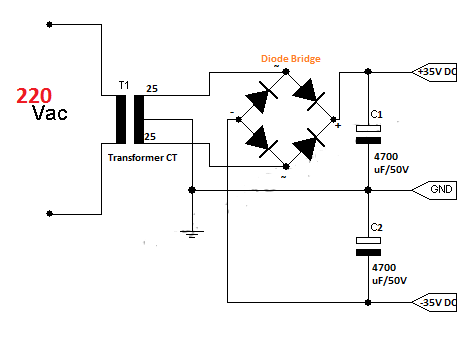
Symmetric Power Supply +35V and -35V Project
Power Supply +12V. -12V and +5V
source : http://datasheetoo.com/power-supply/12v-portable-and-mobile-power-supply-circuit-diagram.html


Monday, 2 July 2012

27MHz Transmitter-Receiver Radio Control PCBs and Schematic Diagram

This article provides information about 27 MHz Transmitter-Receiver Radio Control related to its PCB assembly/construction. The picture below shows the schematic diagram of the transmitter using IC TX2B(TX-2B/RX2B Datasheet).
You will be explained with the instruction for constructing the PCBs (assembly, tuning, transistors, IC, resistors, capacitors (Disk Ceramic, Metallised Polyester, Electrolytic)) for both transmitter (Inductors, LED, Zener Diode, Crystal) and receiver (Zener Diode, Inductors, Resistors, Transistors) with the part value and specifications listed, and how to wiring up the PCBs for both transmitter and receiver.

Find complete description on 27MHz Transmitter-Receiver Radio Control PCBs and Schematic Diagram in this pdf datasheet application (source: scorpiotechnology.com.au).

Remote Control for Home Appliances


Connect this circuit to any of your home appliances (lamp, fan, radio, etc) to make the appliance turn on/off from a TV, VCD or DVD remote control. The circuit can be activated from up to 10 metres. The 38kHz infrared (IR) rays generated by the remote control are received by IR receiver module TSOP1738 of the circuit. Pin 1 of TSOP1738 is connected to ground, pin 2 is connected to the power supply through resistor R5 and the output is taken from pin 3. The output signal is amplified by transistor T1 (BC558). The amplified signal is fed to clock pin 14 of decade counter IC CD4017 (IC1). Pin 8 of IC1 is grounded, pin 16 is connected to Vcc and pin 3 is connected to LED1 (red), which glows to indicate that the appliance is ‘off.’


RF based Wireless Remote Control

This circuit utilises the RF module (Tx/Rx) for making a wireless remote, which could be used to drive an output from a distant place. RF module, as the name suggests, uses radio frequency to send signals. These signals are transmitted at a particular frequency and a baud rate. A receiver can receive these signals only if it is configured for that frequency.

A four channel encoder/decoder pair has also been used in this system. The input signals, at the transmitter side, are taken through four switches while the outputs are monitored on a set of four LEDs corresponding to each input switch.
The circuit can be used for designing Remote Appliance Control system. The outputs from the receiver can drive corresponding relays connected to any household appliance.
Description
This radio frequency (RF) transmission system employs Amplitude Shift Keying (ASK) with transmitter/receiver (Tx/Rx) pair operating at 434 MHz. The transmitter module takes serial input and transmits these signals through RF. The transmitted signals are received by the receiver module placed away from the source of transmission.

The system allows one way communication between two nodes, namely, transmission and reception. The RF module has been used in conjunction with a set of four channel encoder/decoder ICs. Here HT12E & HT12D have been used as encoder and decoder respectively. The encoder converts the parallel inputs (from the remote switches) into serial set of signals. These signals are serially transferred through RF to the reception point. The decoder is used after the RF receiver to decode the serial format and retrieve the original signals as outputs. These outputs can be observed on corresponding LEDs.
Encoder IC (HT12E) receives parallel data in the form of address bits and control bits. The control signals from remote switches along with 8 address bits constitute a set of 12 parallel signals. The encoder HT12E encodes these parallel signals into serial bits. Transmission is enabled by providing ground to pin14 which is active low. The control signals are given at pins 10-13 of HT12E. The serial data is fed to the RF transmitter through pin17 of HT12E.
Transmitter, upon receiving serial data from encoder IC (HT12E), transmits it wirelessly to the RF receiver. The receiver, upon receiving these signals, sends them to the decoder IC (HT12D) through pin2. The serial data is received at the data pin (DIN, pin14) of HT12D. The decoder then retrieves the original parallel format from the received serial data.

When no signal is received at data pin of HT12D, it remains in standby mode and consumes very less current (less than 1µA) for a voltage of 5V. When signal is received by receiver, it is given to DIN pin (pin14) of HT12D. On reception of signal, oscillator of HT12D gets activated. IC HT12D then decodes the serial data and checks the address bits three times. If these bits match with the local address pins (pins 1-8) of HT12D, then it puts the data bits on its data pins (pins 10-13) and makes the VT pin high. An LED is connected to VT pin (pin17) of the decoder. This LED works as an indicator to indicate a valid transmission. The corresponding output is thus generated at the data pins of decoder IC.

A signal is sent by lowering any or all the pins 10-13 of HT12E and corresponding signal is received at receiver’s end (at HT12D). Address bits are configured by using the by using the first 8 pins of both encoder and decoder ICs. To send a particular signal, address bits must be same at encoder and decoder ICs. By configuring the address bits properly, a single RF transmitter can also be used to control different RF receivers of same frequency.

To summarize, on each transmission, 12 bits of data is transmitted consisting of 8 address bits and 4 data bits. The signal is received at receiver’s end which is then fed into decoder IC. If address bits get matched, decoder converts it into parallel data and the corresponding data bits get lowered which could be then used to drive the LEDs. The outputs from this system can either be used in negative logic or NOT gates (like 74LS04) can be incorporated at data pins.
source : http://www.engineersgarage.com/electronic-circuits/wireless-rf-remote-control-circuit
Circuit Diagram

Twitter Delicious Facebook Digg Stumbleupon Favorites More

 
Design by Free WordPress Themes | Bloggerized by Lasantha - Premium Blogger Themes | Bluehost Review